August 4, 2025
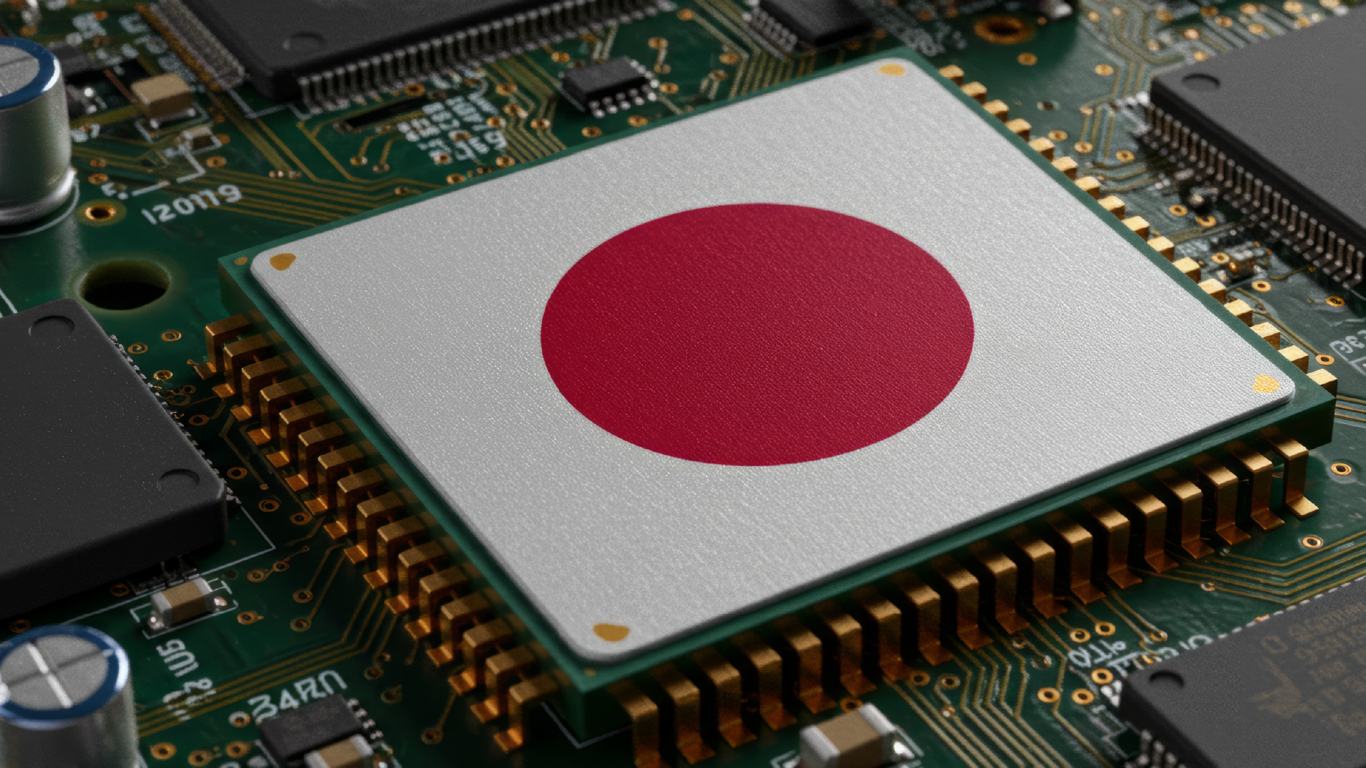
Japan is officially stepping into the race for next-generation semiconductors. In a breakthrough announcement that has sent ripples through the global chip industry, Rapidus Corporation revealed it has successfully prototyped Japan’s first-ever 2nm wafer at its IIM-1 fabrication facility in Chitose, Hokkaido. The wafer is built using the cutting-edge gate-all-around (GAA) transistor architecture, representing one of the most advanced semiconductor nodes ever developed on Japanese soil.
This achievement—realized just months after receiving EUV lithography equipment from ASML—marks a bold re-entry into the highly competitive world of ultra-miniaturized chip production. It also positions Rapidus, and Japan more broadly, as a serious challenger to Taiwan’s longstanding dominance in advanced node manufacturing.
2nm chips represent the next frontier in semiconductor technology. By reducing transistor size while increasing efficiency and density, this node unlocks major performance gains for artificial intelligence, cloud computing, edge devices, and automotive applications. Gate-all-around (GAA) transistors, used in this process, offer better electrostatic control and power efficiency compared to FinFET architectures that dominated previous generations.
Until now, 2nm development has been largely the domain of Taiwan's TSMC, South Korea’s Samsung, and U.S.-based Intel. Rapidus’s entry into this space marks a seismic shift—and a declaration that Japan intends to reclaim its former influence in global chip production.
Rapidus is not just any startup—it is a public-private initiative formed with the express mission of reviving Japan’s semiconductor capabilities. Supported by the Japanese government and a consortium of heavyweight partners—including Toyota, Sony, NTT, NEC, Kioxia, and SoftBank—the company has secured roughly €10 billion in funding to drive its ambitious roadmap.
The IIM-1 site, located in Japan’s northern island of Hokkaido, is envisioned as a flagship facility for cutting-edge manufacturing. Unlike traditional batch processing methods, Rapidus’s strategy employs a single-wafer production model with real-time AI-based optimization for tighter quality control, faster prototyping cycles, and reduced waste.
These milestones not only showcase Rapidus’s speed and agility but also underline Japan’s renewed commitment to semiconductor sovereignty—a concept gaining traction amid escalating geopolitical concerns and supply chain vulnerabilities.
The timing of Rapidus’s achievement is not coincidental. Across the globe, nations are revisiting their semiconductor strategies in response to global disruptions, trade tensions, and the increasing importance of microelectronics in national security.
For Japan, the motivation goes beyond just economics. The country’s long-standing reliance on foreign fabs and offshore foundries exposed it to risks during recent supply chain crises. With Rapidus now producing 2nm wafers domestically, Japan takes a critical step toward securing its future in key sectors such as defense, infrastructure, automotive, and AI.
While Rapidus aims for mass production in 2027, Taiwan’s TSMC has announced it will begin 2nm manufacturing as early as 2025. That means Rapidus still trails the global leader in terms of timeline—but not necessarily in terms of innovation.
The sheer speed with which Rapidus prototyped its first wafer, coupled with its high-profile partnerships and innovative production model, has drawn attention across the semiconductor sector. Industry observers note that while TSMC continues to dominate in scale, newcomers like Rapidus offer more agile and resilient alternatives.
This is especially relevant as chiplets, heterogeneous integration, and energy-efficient architectures become more mainstream. With its AI-driven, single-wafer strategy, Rapidus could play a pivotal role in these emerging paradigms.
Beyond technology, Rapidus’s achievement carries significant geopolitical weight. East Asia remains a focal point for semiconductor tensions, with Taiwan, South Korea, China, and Japan all investing heavily in advanced node capabilities. The United States, for its part, has launched major funding programs to onshore chip manufacturing under the CHIPS Act.
Japan’s resurgence—with Rapidus at the helm—adds another layer to this dynamic. It strengthens supply chain diversification, fosters innovation, and offers like-minded nations an alternative source for critical chip technologies.
In the words of Rapidus CEO Atsuyoshi Koike: “To get here, none of us have slept.” That level of determination—and national alignment—could be Japan’s ace in reclaiming leadership in the chip sector.
The coming years will be critical. As Rapidus transitions from prototyping to production, the firm must navigate challenges around scaling, talent acquisition, ecosystem development, and customer integration. Yet with solid funding, cross-continental collaboration, and strong political backing, the company appears well-positioned.
For Japan, the success of Rapidus could catalyze a broader renaissance in electronics innovation, reinvigorating its standing in a field it once led